


Establishment of Hong Kong's First! Massphoton limited to Establish Hong Kong's First Third-Generation Semiconductor Gallium Nitride Epitaxial Process Global R&D Center
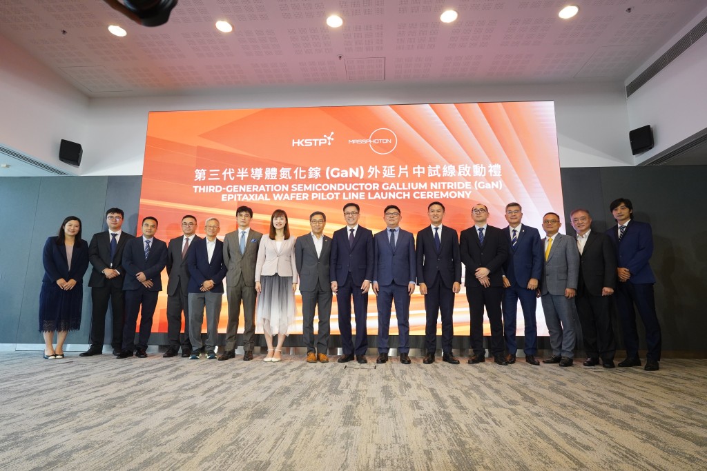
On July 30, Hong Kong Science Park Corporation jointly held the launch ceremony of Hong Kong's first ultra-high vacuum "third-generation semiconductor gallium nitride (GaN) epitaxial wafer pilot line launch ceremony" with MASSPHOTON LIMITED (hereinafter referred to as "our company"). The event aims to promote the development of microelectronics in Hong Kong and further enhance the city's innovation ecosystem.
Leading Technology, Shaping the Future
Our company's CEO, Liu Yitao, said in his speech: "Our company is planning to establish Hong Kong's first third-generation semiconductor gallium nitride epitaxial process global R&D center at Science Park, and open the first ultra-high vacuum mass production-type gallium nitride epitaxial pilot production line at InnoPark. We expect to invest a minimum investment of HK$200 million and establish a research team in Hong Kong, driving the entire third-generation semiconductor industry chain layout."
MASSPHOTON LIMITED currently has a factory in the mainland, founded by a team of overseas-returned semiconductor experts with more than 20 years of technical accumulation and mass production experience in the gallium nitride epitaxy industry. We adopt the world's leading and China-exclusive third-generation semiconductor epitaxy technology with ultra-high vacuum, breaking through the limitations of traditional epitaxy technology and equipment, and successfully producing high-performance gallium nitride optoelectronic and power semiconductor wafers. These wafers are widely used in cutting-edge fields such as healthcare, consumer electronics, Micro-LED displays, photovoltaics, data centers, electric vehicles, rail transit, and ultra-high voltage power transmission. This not only injects strong momentum into enhancing Hong Kong's original research and development standards and new productivity, but also provides the most critical upstream wafer mass production technology support for Hong Kong's semiconductor manufacturing industry chain. Liao Yitao said that the pilot line being deployed in Hong Kong aims to further enhance research and pilot capabilities based on existing mass production levels, especially by combining the existing technologies of Hong Kong's microelectronics experts to ensure global market competitiveness and technological leadership.
The government supports innovation
Government Support Fuels Innovation Innovation, Technology and Industry Bureau Director Sun Dong said that the "Hong Kong Innovation and Technology Development Blueprint" announced by the SAR government includes one development direction of perfecting the innovation and technology ecosystem and promoting Hong Kong's "new industrialization." The government will strongly support advanced manufacturing industries, including the semiconductor industry, in setting up or expanding advanced manufacturing production lines in Hong Kong.
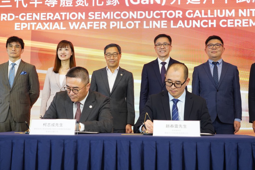
Science Park Corporation CEO Wong Kwok-keung said that Massachusetts Photonic Technology's decision to locate in Science Park and Innovation Park and bring its cutting-edge technology and experience to Hong Kong will be an important milestone in Hong Kong's microelectronics industry and "new industrialization" journey. He also said that Science Park has been cooperating with the government to fully develop the microelectronics industry, with over 200 park companies engaged in the industry. He hopes to enhance Hong Kong's microelectronics R&D capabilities and industrialization, and help Hong Kong become an international innovation and technology hub. On the day, the signing ceremony was witnessed by the Director of Innovation and Technology and Industry, Mr. Sun Dong; the Deputy Director of Innovation and Technology and Industry, Ms. Zhang Manli; the Vice President of the Office of Important Enterprise Introduction (Advanced Manufacturing and New Energy Technology), Mr. Wang Guofan; the Chief Executive Officer of Hong Kong Science Park Company, Mr. Wong Kek-cheong; the Chief Executive Officer of MASSPHOTON LIMITED, Mr. Liao Yi-tao; and shareholders and investors of MASSPHOTON LIMITED, Mr. Wong Yung-yiu. The agreement was signed by Mr. Kao Chi-shing, the Acting Chief Business Development Director and Chief Business Development Director of the Innovation and Technology Ecosystem of Hong Kong Science Park Company, and Mr. Zhao Chun-lei, the Chief Marketing Officer of MASSPHOTON LIMITED.
Establishing a Presence in Hong Kong and Focusing on Talent
Our Chief Executive Officer, Mr. Liao Yi-tao, stated that we plan to move into the newly built Hong Kong Science Park Microelectronics Center (MEC) and establish Hong Kong's first 8-inch gallium nitride (GaN) epitaxial wafer research and pilot production line. We will also collaborate with the Hong Kong Microelectronics Research Institute (MRDI) to develop downstream gallium nitride optoelectronics and power devices based on our epitaxial wafers. Through the development and incubation of new products, we aim to establish a cutting-edge and comprehensive patent portfolio for ultra-high vacuum gallium nitride epitaxy technology and products. Within three years, we will complete the pilot line and initiate the construction of gallium nitride epitaxy production lines in Hong Kong, launching Hong Kong-made epitaxial wafers into the global market.
Choosing to establish our global R&D center and pilot line in Hong Kong is a strategic move that we believe will enable us to grow in a technologically advanced, talent- and capital-intensive international environment. We plan to recruit PhD graduates and professionals specializing in semiconductor development in the future. We also believe that Hong Kong's unique advantage in cross-cultural exchange will help us launch Hong Kong-made epitaxial wafers into the global market. Additionally, Hong Kong's international features and talent pool make it an irreplaceable hub for global markets, regardless of what type of products are ultimately produced. Therefore, we will pay special attention to talent in Hong Kong in all areas, including research and development, product development, and marketing.
The strategic move by Massachusetts Photonic Technology to establish a global R&D center and pilot line in Hong Kong not only injects new vitality into Hong Kong's microelectronics industry but also contributes new forces to global technological progress and economic development. We have every reason to believe that, with its outstanding R&D capabilities and innovative spirit, Massachusetts Photonics will lead the gallium nitride semiconductor industry to an even more brilliant future in the near future. At the same time, the successful implementation of this project will further promote the development of Hong Kong's innovative technology ecosystem and inject strong momentum into Hong Kong's long-term development.